

Solid-state amplifiers have superior technical specifications compared to valve/tube amplifiers but when solid-state amplifiers were first introduced it was noticed that they sounded flat and lifeless in comparison to well made valve/tube amplifiers. Also a solid-state amplifier had to be twice as powerful as a valve/tube amplifier to sound as loud - Why? Unfortunately little to no research was done.
Amplifiers and speakers have traditionally been marketed and sold independently of each other. There has been little interest in how amplifiers and speakers interact. Valve/tube technology was tediously assembled with manual labour whereas solid-state technology is mass produced at a fraction of the cost. Economical rationalism and modern marketing easily pushed aside the older valve/tube technology. Page 8 has a detailed explanation of voltage-drive and current-drive, which enables us understand why valve/tube and solid-state amplifiers sound so different.
Basic technical principles
Many professional audio providers and audiophiles have misconceptions about how a solid-state (transistor) amplifier functions. Misconceptions occur because basic principles are not understood. Please be attentive when reading these pages as each step adds to the next and becomes complex very quickly. If a step becomes difficult to understand, take time to review the previous steps.
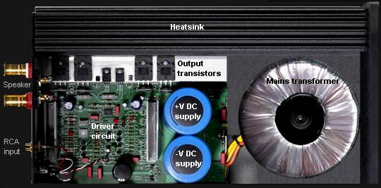
A solid-state amplifier consists of 3 sections.
1 The input driver circuit amplifies the small input signal to a larger size, approx x20 to x50.
2 The large output transistors add current to the amplified signal to be sent to the speaker.
3 The power supply converts 110V / 22OV AC mains to 2 DC supply Voltages that power the amplifier.
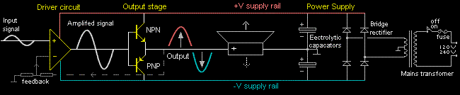
The principles of each section will be described, beginning with the output stage. The output stage consists of 2 or more large output transistors bolted to a heat sink (NPN and PNP).
A solid-state amplifier has 2 (DC) power supplies (+V and -V). The 2 power supplies are connected in series. The middle is connected to the chassis. One terminal of the speaker is connected to the middle chassis and other speaker terminal is switched between the 2 supplies. We shall begin with batteries as the power supply.
As the speaker is connected from the chassis across the +V supply, the cone moves out.
As the speaker is connected from the chassis across the -V supply, the cone moves in.
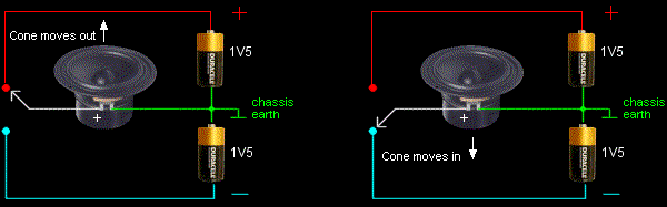
The speaker is connected across one power supply at a time. Therefore, the maximum voltage across the speaker can be no greater than 1V5 at any one point in time.
Note - In electronic circuits we try not to use decimal points (1.5V) because grammatical full stops and cockroach droppings .... are the same size .... 1.5V is written as 1V5
Speaker polarity. One of the terminals on the speaker has a polarity + identification mark. The + symbol identifies which terminal has to be connected to a +V to cause the cone to move out. In stereo systems or paralleling speakers it is essential that all speakers move together (in and out) in the same direction. When only 1 speaker is used as mono it makes no difference which way around the speaker terminals are connected.
We must redraw the same circuit and remember the correct symbols and names for each part of the circuit. Circuit drawings do not use colour. The colour in the pics is for temporary assistance only.
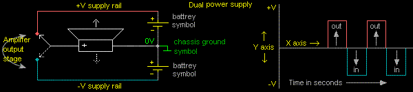
- Dual power supply
- Battery long line is + short line is -
- Supply rails +V and -V from the dual power supply.
- Chassis and ground symbol is 0V
- Graph Y axis is the dual power supply Voltage, X axis is time.
- Graph shows the + - V switched to the speaker over time.
The speaker is not directly switched on and off between the 2 power supplies but gradually connected to each power supply in turn through solid-state devices that behave as variable resistors, in a way that follows the audio signal. These solid-state devices behave as transfer resistors, therefore are named 'transistors'.
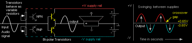
The output transistors swing the speaker between the +V supply then to the -V supply, in-sympathy with the music. The output transistors provide current from the + - V supply rails to drive the speaker. Output transistors do not increase the size of the music signal. The output transistors behave as variable resistors conducting current from each power supply in turn and get hot, very hot. They are bolted to a large piece of aluminium with fins (heat-sink). Heat is the enemy of transistors. The maximum power output of an amplifier is dependant on the current and voltage from the power supplies.
NPN and PNP transistors are polarity complements of each other. PNP is positive-negative-positive and vice-versa. The input signal has to reach 0.65V (650mV) before each transistor will start to conduct. This means there is a total gap of 1V3. This gap is named 'crossover distortion' and was a major problem of solid-state amplifiers when they were first introduced. It took many years before this problem was correctly solved.
Transistors and diodes
The cathode K of a diode and the emitter of a transistor have an arrow head symbol. The arrow head points (forward) to the -V of a battery or voltage supply in the circuit for the diode or transistor to function.
A circuit is a circle, so it does not matter where in the circle each item is placed. It is easier to read a circuit if everyone draws it the same way and places the power supply vertically on the right, with +V at top and -V at bottom. Switch, diode, transistor or control circuit at left.
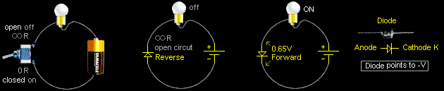
The left side of the above pic shows a battery, light bulb and switch. & When the switch is open, the resistance across the switch is infinite ∞R. When switch is closed the resistance across the switch is zero 0R.
∞ Resistance can be described as an open circuit (infinite resistance).
0 Resistance can be described as a short circuit.
A diode acts as a open circuit if the arrow points toward the +V in the circle (reverse).
A diode acts as a short circuit if the arrow points toward the -V in the circle (forward).
In the forward direction a diode requires 0.65V (650mV) across it to activate. Less than 0.65V (650mV) the diode will be an open circuit. An activated diode it will remain locked at 0.65V across it, regardless of the amount of current the diode conducts. Therefore, a diode will get slightly hot as the current increases.
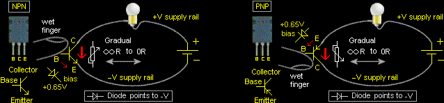
The diode is replaced with an NPN transistor on the left and a PNP transistor on the right. NPN and PNP transistors are polarity complements of each other, which enables them to be used from a +V or -V supply. A transistor can be made to behave as a resistor that changes its value between an open circuit (∞ resistance) to almost a short circuit (0R), therefore controlling the brightness of the light bulb.
By placing a finger on the base causes a very small amount of current between the base and emitter, which will then enable a larger amount of current to flow between the collector and emitter - enabling the brightness of the light bulb to be adjusted. Notice that the red arrows are symbolising that the transistors are actively functioning, whereas the transistor emitter arrow head points to the -V in the circuit to represent the correct polarity for it to function. A small amount of current between the base and emitter enables a larger amount of current between the collector and emitter.
HFE (hybrid forward emitter) is a technical term to describe the current gain of a transistor. The HFE (gain) of a transistor increases with temperature but decreases with current, which makes it difficult to control. Small signal transistors can have a HFE (gain) of 100 to 200, whereas large power transistors will have a low HFE of approx 20 to 100.
Bias 0.65V (650mV). The transistor junction between base and emitter acts like a diode. Nothing will happen until 0.65V (650mV) is reached between the base and emitter, only then is the transistor activated. When the bias of 0.65V is reached the transistor is activated and the base_emitter will always be locked together at 0.65V (650mV). Therefore, the emitter of the transistor in an amplifier will always follow the input signal on the base (less the 0.65V bias) with added current from the collector.
Review the previous steps.
N.B. Bias voltages of diodes, transistors and amplifier designs are generalised in this text. Detailed engineering reference for electronic components and amplifier design can be found on
sound-au.com
wikipedia.org / Transistor
wikipedia.org / Bipolar Transistor
Output stage, class B and class AB
Crossover. Each transistor controls each half of the sine wave. This is described as Class B. The crossover gap is 650mV and 650mV across each base_emitter. Eliminating the crossover gap between each half of the audio signal is the most critical part of solid-state amplifier design. The distortion created by the crossover gap generates an annoying 1/3 harmonic sound imposed in the music, similar to the sound of tearing paper. A reduced gap of 1/000V (1mV) is still audible. The gap must be closed, plus the current through each transistor must slightly overlap the other to insure there can be no crossover gap.
A bias string using 2 diodes is placed before the output transistors so 650mV + 650mV is already causing each of the output transistors to be activated with quiescent current flowing between the collector and emitter. This quiescent bias current closes the 650mV gap of each transistor. Some amplifiers use 2 diodes in a string, but the majority have a more complex circuit that allows the quiescent current (overlap) to be adjusted.

Providing the gap is closed with a small quiescent current through the output transistors to provide a small overlap, the crossover distortion is eliminated. Quiescent current generates waste heat in the output transistors, approx 3 to 5W per transistor. This waste heat is also described as the quiescent temperature. A High-powered amplifier with many output transistors will create a lot of quiescent heat and need to be fan cooled. There is a R47 (0.47R ) resistor in series with each emitter. Emitter resistors help stabilise the quiescent current. They are physically large and have a very low resistance 1/2R approx.